
Graphene Based Radar Absorbing Materials
Engineering materials that reduce reflected electromagnetic energy
GTechPlasma develops plasma-synthesised graphene, nitrogen-doped graphene and functional graphene-based materials for radar and microwave absorption. We tune electrical and dielectric behaviour, loss mechanisms and material architecture so that electromagnetic energy can enter the tested structure, be attenuated within it and return less energy toward the source.
Graphene and N-graphene
|
Absorption-oriented design
|
Broadband characterisation
|
Application-led integration
|
Graphene and N-graphene | Absorption-oriented design | Broadband characterisation | Application-led integration |
What radar absorbing materials are
What is a radar absorbing material
A radar absorbing material, or RAM, is a material or multilayer structure designed to reduce electromagnetic energy reflected toward a radar or microwave source under defined conditions. A useful absorber combines limited front-surface reflection with sufficient internal attenuation. Its performance depends on frequency, thickness, backing, substrate, incidence angle, polarisation, geometry and installation. A reflection-loss value therefore describes a tested specimen and configuration, not a powder or filler in isolation.
How absorption is created
| Design function | What it must achieve | Variables to control |
|---|---|---|
| Energy entry | Limit the impedance discontinuity at the incident surface so that useful power enters the structure. | Complex permittivity and permeability, conductivity, surface layer, porosity and thickness. |
| Internal attenuation | Dissipate accepted energy through electrical, dielectric, interfacial and, where present, magnetic loss. | Graphene network, defects, interfaces, dopants, complementary phases and propagation path. |
| Return suppression | Prevent coherent energy from propagating back out of the structure. | Loss, phase, layer order, backing, interfaces, geometry and manufacturing quality. |
High conductivity alone is not enough. A very conductive surface can reflect strongly before energy enters the absorber. Low reflection requires a balance between impedance matching and attenuation, engineered for the target band and the complete material stack.
Engineering dielectric magnetic synergy
High attenuation alone does not guarantee low reflection. Effective absorbers must combine sufficient internal loss with an impedance profile that allows electromagnetic energy to enter the material. GTechPlasma uses nanoscale engineering and multiphase hybridisation to tune dielectric and magnetic loss mechanisms together, creating additional degrees of freedom for balancing impedance matching and attenuation.
Complementary functional phases can perform different electromagnetic roles. Depending on the formulation, they can modify impedance matching, interfacial polarisation, dielectric loss, eddy-current-related loss and magnetic resonance mechanisms. The objective is to engineer the combined response, without disclosing proprietary precursor ratios or phase compositions.
How radar absorption is measured
Reflection loss and effective absorption bandwidth
Reflection loss is commonly reported in decibels for a defined measurement reference plane. More negative reflection loss indicates a smaller returned field magnitude in that configuration. An RL of −10 dB corresponds to ten per cent reflected power under the applicable assumptions. For a metal-backed specimen, transmission is approximately zero; for a transmitting specimen, absorption must be calculated from both reflected and transmitted power.
Effective absorption bandwidth, or EAB, is the continuous frequency interval over which reflection loss remains below a declared threshold, commonly −10 dB. The threshold, band limits, specimen thickness, backing, incidence, polarisation and measurement method must be published with the value. Results from different thicknesses or formulations must not be combined and described as one specimen's bandwidth.
Measured from calibrated scattering parameters
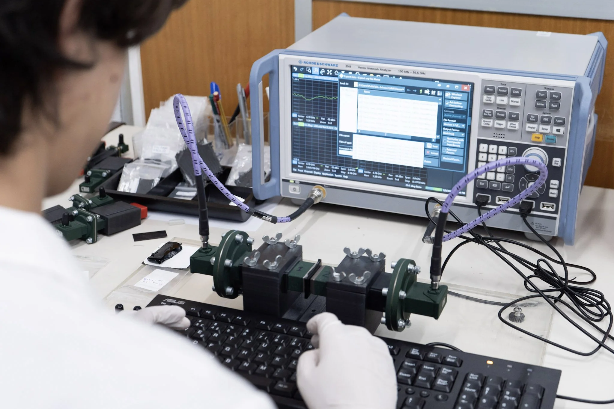
Electromagnetic response is characterised using vector network analyser measurements and appropriate waveguide or free-space configurations. Calibrated complex S-parameters are used to derive reflection, transmission and absorption, while reflection loss and EAB are reported with the specimen, reference plane, thickness, backing and frequency interval needed to interpret them.
| Metric | What it answers | Required context |
|---|---|---|
| Reflection loss | How much field is returned by a stated absorber configuration. | Sample, thickness, substrate, backing, method, reference plane, frequency and uncertainty. |
| EAB | The continuous interval meeting the declared reflection-loss threshold. | Threshold, endpoints, sample, thickness and full test conditions. |
| R, T and A | How incident power is partitioned into reflection, transmission and absorption. | Calibrated S-parameters, measurement geometry and calculation convention. |
| Radar cross section | How strongly a complete object scatters toward a radar under stated conditions. | Integrated geometry, frequency, aspect, polarisation, configuration, measurement or validated simulation. |
Why graphene and N-graphene
Graphene as an electromagnetic design component
Graphene combines low density, high aspect ratio, electrical transport and extensive interfacial area. In coatings, polymers and porous structures, it can form controlled conductive pathways and create heterogeneous interfaces that contribute to conduction loss, charge accumulation and dielectric relaxation. The result depends on graphene grade, morphology, defect state, dispersion, loading, matrix and processing; the name graphene alone does not specify absorber performance.
Controlled conductive networks can provide attenuation without automatically maximising surface reflection.
Large interfacial area can support interfacial polarisation and distributed relaxation processes.
Defects, edges and surface chemistry provide additional variables for dielectric response.
Low-mass coatings, foams, films and composites can be designed when the complete formulation preserves the weight advantage.
Nitrogen doping for tunable response
Nitrogen doping changes graphene's electronic and defect structure. Nitrogen content and bonding configuration can alter carrier behaviour, local dipoles, polarisation sites and complex permittivity, providing an additional route to balance loss and impedance matching for a selected frequency range. The effect is formulation- and frequency-dependent and must be measured in the final architecture.
Nitrogen-containing configurations, including pyridinic and pyrrolic environments, can act as polarisation centres. Together with structural defects and heterogeneous interfaces, they introduce dipolar and interfacial relaxation pathways under an alternating electromagnetic field. These mechanisms provide another design variable for tuning loss while preserving the impedance conditions required for energy entry.
GTechPlasma's scientific base includes continuous atmospheric-pressure microwave-plasma synthesis of graphene and N-graphene and frequency-dependent tuning of dielectric permittivity. This supports the materials-design approach; it does not replace performance data for a finished coating, coupon or component.
Why absorption-oriented shielding requires more than conductivity
The GTechPlasma approach
From target band to validated material architecture
GTechPlasma treats radar absorption as a coupled materials-and-integration problem. The objective is not the powder with the highest conductivity or the coupon with the deepest isolated minimum. It is a reproducible architecture that meets the required band, reflection threshold, thickness, mass, substrate, environment and manufacturing constraints.
Define the requirement: frequency range, reflection threshold, angle and polarisation range, substrate, geometry and environment.
Select or tailor the plasma-synthesised graphene or N-graphene building block, including morphology, defect state, doping and matrix compatibility.
Engineer the architecture through loading, dispersion, layer sequence, porosity, gradients, backing and complementary phases where justified.
Characterise constituents and coupons using composition, electrical properties, complex permittivity and permeability where relevant, S-parameters, reflection loss and R, T and A.
Validate the representative configuration, including substrate, interfaces, curvature, seams, production tolerances and application-relevant incidence conditions.
AEGIS electromagnetic materials
AEGIS stands for Advanced Electromagnetic Graphene-based Shields via Plasma Induced Synthesis. Publicly associated with the NATO Science for Peace and Security Programme, AEGIS provides an engineering platform for lightweight graphene-based electromagnetic materials. For radar-absorption work, its relevance lies in tunable formulations that balance energy entry and internal attenuation for defined bands and structures.
Electromagnetic performance has been experimentally characterised from 5 to 70 GHz across the GTechPlasma material portfolio. This range is covered by different formulations and test configurations; it must not be read as continuous 5–70 GHz performance from every AEGIS material. Approved results should be presented formulation by formulation, with the conditions that produced them.
Tunable by formulation, not just thickness
Broadband absorption is often pursued by changing absorber thickness or filler loading between bands. The reported N-graphene hybrid study demonstrates another design dimension: different nanostructures and complementary phases produced distinct electromagnetic responses while retaining a common 2 mm specimen thickness and 15 wt% filler content.
This formulation-dependent tuning shifted effective absorption behaviour across the C, Ku, Ka and V bands. Reported EAB values were approximately 2.1 GHz in C, 3.4 GHz in Ku, 8 GHz in Ka and 4 GHz in V; each value belongs to the identified formulation and test configuration and must not be combined into a claim for one universal material.
GTechPlasma's position is therefore specific and defensible: plasma synthesis creates graphene and N-graphene building blocks whose composition and electromagnetic properties can be tailored; AEGIS combines those building blocks with application-specific material architectures and validation.
One plasma environment. Multiple nanoscale processes.
The microwave plasma environment can simultaneously drive N-graphene formation, nanoparticle generation, surface functionalisation, multiphase formation and nanoparticle anchoring onto the graphene scaffold. This integrated route creates hierarchical hybrid structures without relying on a sequence of separate wet-chemical synthesis and functionalisation steps.
From plasma parameters to measured performance
Plasma parameters → N-graphene chemistry, defects and interfaces → particle size, distribution and phase → dielectric and magnetic response → impedance matching and attenuation → reflection, transmission and absorption.
This structure to property to performance chain describes GTechPlasma as a plasma-enabled materials-engineering platform: synthesis controls nanostructure and loss mechanisms, while measurements determine whether the resulting architecture meets the target band and integration conditions.
Material absorption and radar cross section
A strong coupon result is not a platform claim
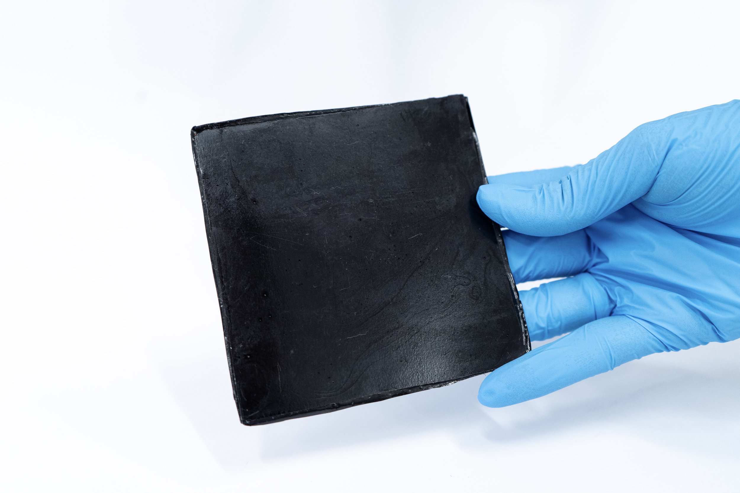
Material or coupon measurements describe reflection, transmission and absorption for a defined specimen. Radar cross section describes scattering from a complete object and depends additionally on shape, size, edges, cavities, seams, apertures, joints, substrate, aspect, polarisation and observation geometry. A strong coupon result supports integration work; it does not prove a stated platform-level RCS reduction.
From material performance to platform validation
Promising absorber performance must be validated on representative substrates, geometries and components before progressing to full-platform assessment. This staged approach connects material-level electromagnetic performance with the practical objective: reducing reflected energy where it matters in the final system.
| Question | Material or coupon absorption | Platform-level radar cross section |
|---|---|---|
| What is measured | Reflection and, where relevant, transmission from a defined specimen. | Scattered field or power from the integrated object under stated observation conditions. |
| Typical evidence | S-parameters, RL curves, R, T and A, constitutive properties and uncertainty. | Calibrated range measurement or validated full-object simulation versus frequency, aspect and polarisation. |
| Defensible conclusion | The tested material stack reduced reflection under the stated conditions. | The integrated object produced the reported RCS under the stated conditions. |
| Claim boundary | Do not convert coupon RL or EAB into a platform RCS figure. | Do not generalise one geometry, aspect or configuration to all operating conditions. |
EMI shielding and radar absorbing materials
Related physics with different primary objectives
EMI shielding primarily reduces electromagnetic transmission or coupling through a material, component or enclosure. Radar absorbing materials primarily reduce the energy returned toward a radar receiver in a relevant geometry, band, polarisation and angle range. A highly reflective conductor can therefore provide excellent EMI shielding while remaining a poor low-reflection radar absorber.
GTechPlasma develops materials relevant to both domains, but the metrics and claims should remain separate. The electromagnetic-shielding authority page explains shielding effectiveness and the R, T and A power balance. This page focuses on reflection loss, effective absorption bandwidth, material integration and the evidence required before an RCS claim.
Applications
Aerospace and unmanned systems
Lightweight coatings and composite architectures may be evaluated where reflection control must be balanced with mass, thickness, aerodynamics and environmental durability. Validation should use representative substrates and include curvature, temperature cycling, moisture, fluids, vibration, coating repair and manufacturing tolerance.
Defence and security systems
Potential uses include antenna integration, protected electronics, housings and electromagnetic-signature materials. Public content should describe material capabilities and validation routes without disclosing restricted details or implying a platform outcome from coupon data.
Antenna and radio frequency engineering
Absorbers can help control cavity modes, unwanted coupling, back radiation and local reflections around antennas and test fixtures. Component validation must consider the field regime, power level, thermal load, geometry and impact on antenna efficiency.
Microwave test mobility and communications
Test structures, radar-equipped vehicles and high-frequency electronics can require stable local reflection control. Relevant constraints include production tolerance, temperature, vibration, humidity, compression, adhesives, fire behaviour and long-term dimensional stability.
Technical frequently asked questions
Can graphene absorb radar waves
Yes, when it is incorporated into a suitable architecture. Graphene can contribute conduction loss, interfacial polarisation and defect-related relaxation. Whether the finished specimen is absorptive or strongly reflective depends on conductivity, loading, dispersion, thickness, matrix, backing and frequency.
Why is maximum conductivity not always desirable
Very high conductivity can increase the impedance mismatch at the incident surface and return more energy before it enters the material. A low-reflection absorber needs a controlled balance between energy entry and internal attenuation.
What does a reflection loss of - 10 dB mean
Under a properly calibrated measurement, −10 dB corresponds to ten per cent reflected power at the stated frequency and reference plane. It does not automatically mean ninety per cent absorption if the specimen transmits power. For a metal-backed specimen, transmission is approximately zero.
What is effective absorption bandwidth
EAB is the continuous frequency interval over which reflection loss meets a declared threshold, commonly below −10 dB. It is meaningful only with the specimen, thickness, backing, method, incidence and polarisation.
How does thickness affect radar absorption
Thickness changes propagation distance and phase, so it can move reflection minima and alter attenuation. A thicker absorber is not automatically better. Publish separate curves for each measured thickness.
What can nitrogen doping change
Nitrogen incorporation can alter carrier behaviour, defects, dipoles and complex permittivity. It may help tune dielectric loss or matching in a particular architecture, but the result depends on composition, frequency and matrix and must be measured.
Does a good coupon result guarantee radar cross section reduction
No. Coupon reflection loss describes one material stack under defined laboratory conditions. Platform RCS also depends on geometry, edges, gaps, cavities, joints, aspect, polarisation and observation geometry. Integrated measurement or validated full-object simulation is required.
What should a technical data request include
Provide the target frequency range, acceptable reflection level, maximum thickness and areal density, substrate and geometry, environmental exposure, incidence and polarisation range, production scale and qualification constraints.
Scientific evidence
Xia Y, Gao W and Gao C. A Review on Graphene-Based Electromagnetic Functional Materials: Electromagnetic Wave Shielding and Absorption. Advanced Functional Materials 32, 2204591 (2022). https://doi.org/10.1002/adfm.202204591
Tatarova E et al. Plasma-Driven Tuning of Dielectric Permittivity in Graphene. Small 20, 2303421 (2024). https://doi.org/10.1002/smll.202303421
Dias A I A et al. Plasma-enabled multifunctional platform for gram-scale production of graphene and derivatives. Applied Materials Today 36, 102056 (2024). https://doi.org/10.1016/j.apmt.2024.102056
Bundaleska N et al. Microwave Plasma-Driven Synthesis of Graphene and N-Graphene at a Gram Scale. Processes 13, 196 (2025). https://doi.org/10.3390/pr13010196
IEEE Standards Association. IEEE 1502 Recommended Practice for Radar Cross-Section Test Procedures.
Materials engineered for controlled microwave interaction
GTechPlasma combines plasma synthesis, graphene science and electromagnetic materials engineering to develop absorber systems for defined frequency ranges and integration conditions. The work starts with measurable material properties and continues through architecture, processing, characterisation and representative-component validation.
The differentiator is a plasma-enabled materials-engineering platform that controls nanostructure, interfaces and coupled loss mechanisms to tune electromagnetic absorption by formulation, not only by thickness.
The objective is precise: allow electromagnetic energy to enter the tested structure, attenuate it through controlled loss mechanisms and reduce the energy returned from its surface. Where a programme requires platform-level radar-cross-section performance, material development must be followed by geometry-aware modelling and integrated measurement.