
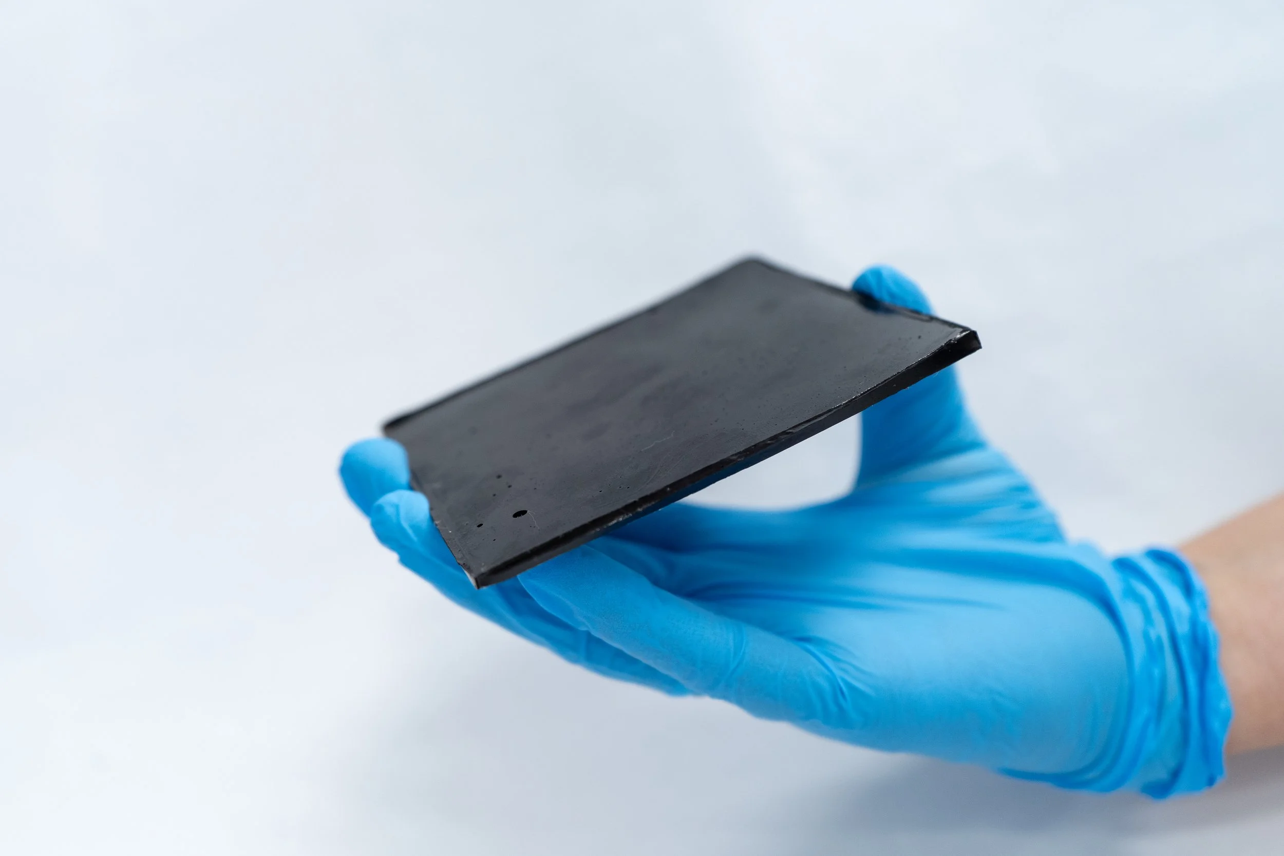
Graphene Based Electromagnetic Shielding and Absorption
Engineering electromagnetic interaction through advanced graphene materials
GTechPlasma develops plasma-synthesised graphene, nitrogen-doped graphene and functional graphene-based materials for electromagnetic shielding and absorption. By controlling composition, structure and material architecture, we work to balance electrical transport, dielectric response, impedance matching and attenuation so that electromagnetic energy can be dissipated within a material rather than simply redirected at its surface.
Graphene and N-graphene
|
Absorption-dominant design
|
Tunable electromagnetic properties
|
Broadband characterisation
|
Graphene and N-graphene | Absorption-dominant design | Tunable electromagnetic properties | Broadband characterisation |
What electromagnetic interference shielding is
What is electromagnetic interference shielding
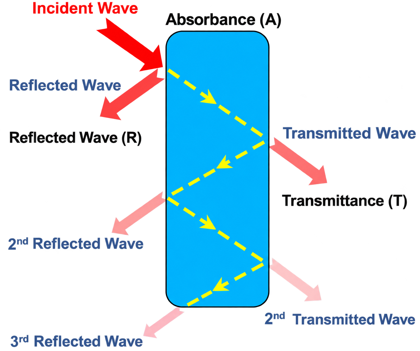
Electromagnetic interference shielding is the reduction of electromagnetic power transmitted from one side of a material, component or enclosure to the other. When an incident wave reaches a shield, some power is reflected, some is absorbed and dissipated within the material, and some is transmitted. The balance depends on frequency, thickness, geometry, electrical conductivity, complex permittivity, complex permeability, interfaces and the surrounding medium. A valid shielding result therefore belongs to a defined specimen and test configuration; it is not an intrinsic number that can be transferred unchanged to every product design.
Shielding protects systems by controlling unwanted coupling. Depending on the application, this may mean limiting emissions from electronics, protecting sensitive circuits from external fields, reducing crosstalk, or controlling electromagnetic leakage through a structure. The required method and performance threshold depend on whether the object under test is a planar material, a cable, a component, an enclosure or a complete platform.
How incident power is partitioned
$$ R + A + T = 1 $$
Here R is the reflected power fraction, A is the absorbed power fraction and T is the transmitted power fraction. These coefficients must be defined on a power basis and under stated measurement conditions. They provide the clearest physical description of what happens to the incident wave at the tested reference plane.
| Outcome | Physical meaning | Design relevance |
|---|---|---|
| Reflection | Power returned toward the incident side because the wave encounters an impedance discontinuity. | Can reduce transmission, but may create reflected fields that matter elsewhere in the system. |
| Absorption | Power dissipated inside the specimen through electrical, dielectric, magnetic and interfacial loss processes. | Important when low reflection or controlled dissipation is part of the requirement. |
| Transmission | Power that emerges on the far side of the specimen in the measured propagation path. | The main quantity reduced by an EMI shield. |
| Internal interactions | Repeated scattering, reflection and propagation inside pores, layers and interfaces. | Can increase path length and attenuation, although its treatment in shielding equations depends on the adopted formulation. |
Shielding effectiveness
$$ SE_T = -10 \log_{10}(T) $$
Total shielding effectiveness, SE_T, expresses transmission attenuation in decibels. For example, 20 dB corresponds to one per cent power transmission in the tested configuration, while 30 dB corresponds to 0.1 per cent. These examples describe transmission only; they do not reveal how much of the incident power was reflected or absorbed.
$$ SE_T = SE_R + SE_A $$
In the widely used scattering-parameter calculation convention, total shielding effectiveness is decomposed into reflection and absorption terms. In classical treatments, a multiple-reflection term may also be written. The naming can cause confusion: SE_R and SE_A are logarithmic contributions to transmission loss and must not automatically be interpreted as the actual reflected and absorbed fractions of incident power. For any claim of absorption-dominant behaviour, report R, A and T directly and state the calculation convention.
Reflection dominant and absorption dominant shielding
Two materials can produce similar total shielding effectiveness while interacting with the incident field in very different ways. A conductive surface may reject most power at its front face. A lossy, better-matched structure may admit more power and dissipate a larger fraction internally before little remains available for transmission. The preferable response depends on the system requirement.
Scientific definition of absorption dominated shielding
An absorption-dominated shield is engineered so that a substantial fraction of incident electromagnetic energy enters the material rather than being immediately reflected. Once inside, that energy is attenuated through conduction, dipolar and interfacial polarisation, defect-related relaxation and, where present, magnetic loss mechanisms. The claim must be demonstrated from the measured power fractions R, T and A over the stated range and configuration, not inferred from SE_A and SE_R alone.
| Design question | Reflection-dominant response | Absorption-dominant response |
|---|---|---|
| Primary interaction | A large share of incident power is returned toward the source side. | A large share of incident power enters and is dissipated within the tested structure. |
| Typical route | High conductivity and strong impedance discontinuity. | Controlled input impedance combined with sufficient internal attenuation. |
| Potential benefit | High transmission attenuation with a simple conductive barrier. | Lower returned power where reflection control matters. |
| Potential limitation | Reflected fields may couple into nearby systems or alter the electromagnetic environment. | Performance can be sensitive to thickness, interfaces, frequency and incidence conditions. |
| Evidence to publish | SET with R, A and T, plus thickness and test method. | R, A and T with SET, bandwidth, thickness and uncertainty; angle and polarisation where relevant. |
Technical point. A result for $ SE_A $ that exceeds $ SE_R $ does not by itself prove that more incident power was absorbed than reflected. Use the power coefficients to make that statement.
Visual guide: Reflection vs Absorption in Electromagnetic Shielding
Why graphene
Why graphene is relevant to electromagnetic shielding
Graphene is relevant because a small mass of high-aspect-ratio conductive material can form extended electrical pathways and a large interfacial area inside a coating, polymer or porous structure. Those pathways can support conduction loss, while defects, edges, functional groups and heterogeneous interfaces can contribute polarisation and relaxation processes. The resulting response depends on graphene quality, morphology, dispersion, orientation, loading, matrix and processing; the word graphene alone does not specify electromagnetic performance.
Electrical transport. Connected graphene networks can support mobile charge and ohmic dissipation. The percolation threshold and conductivity depend strongly on flake structure, contact resistance, orientation and dispersion.
Dielectric response. Charge accumulation at defects, boundaries and heterogeneous interfaces can create frequency-dependent polarisation and dielectric loss.
Interfacial area. Graphene introduces extensive interfaces with polymers and other functional phases, creating opportunities to tune charge accumulation and relaxation.
Low density and high aspect ratio. Graphene can contribute to lightweight, thin or flexible architectures when the complete composite and manufacturing process preserve those advantages.
Architectural flexibility. Graphene can be used in films, coatings, foams, laminates, textiles, polymer composites and hybrid structures, each with a different balance of conductivity, matching and attenuation.
Why higher conductivity is not always better
Raising conductivity can improve transmission attenuation, but it can also increase the mismatch between free space and the material surface. A stronger mismatch generally increases front-surface reflection and reduces the power available for internal dissipation. For an absorption-dominant design, conductivity must be considered together with complex permittivity, complex permeability, thickness, microstructure and the target frequency range. The engineering objective is not maximum conductivity in isolation. It is the electromagnetic response required by the application.
Why nitrogen doped graphene
N-graphene for an engineered electromagnetic response
Nitrogen doping modifies the electronic and defect structure of graphene. The amount, bonding configuration and distribution of nitrogen can alter carrier behaviour, local dipoles, polarisation sites and complex permittivity. These changes may help tune dielectric loss and impedance matching, but the direction and magnitude of the effect depend on synthesis, composition, frequency and the surrounding material architecture. N-graphene should therefore be characterised as a defined material, not treated as a universal performance upgrade.
Nitrogen-containing configurations, including pyridinic and pyrrolic environments, can behave as polarisation centres. Together with defects and heterogeneous interfaces, they create dipolar and interfacial relaxation pathways when the alternating field changes faster than the local dipoles can follow. Nitrogen doping therefore adds a controllable mechanism for dielectric loss as well as changing conductivity, but its benefit must be verified in the complete composite.
Published work associated with GTechPlasma's scientific base reports atmospheric-pressure microwave-plasma routes for the continuous synthesis of free-standing graphene and N-graphene, including control over structural properties and nitrogen incorporation. Related research has demonstrated tunable dielectric permittivity in plasma-synthesised nitrogen-doped graphene across microwave frequencies. These findings support a material-design strategy in which doping is used to adjust electromagnetic behaviour, while application performance remains subject to formulation and validation in the final architecture.
Engineering electromagnetic absorption
Complex permittivity and permeability
$$ \begin{aligned} \varepsilon_r &= \varepsilon' - j\varepsilon'' \\ \mu_r &= \mu' - j\mu'' \end{aligned} $$
The real components ε′ and μ′ describe electric and magnetic energy storage under the adopted sign convention. The imaginary components ε″ and μ″ describe dielectric and magnetic dissipation. For many graphene-polymer systems, dielectric behaviour dominates unless a magnetic phase is deliberately introduced. Claims of magnetic loss should be supported by composition and frequency-dependent permeability data.
$$ \begin{aligned} \text{electric loss tangent} = \frac{\varepsilon''}{\varepsilon'} \\ \text{magnetic loss tangent} = \frac{\mu''}{\mu'} \end{aligned} $$
Loss tangents help describe the balance between dissipative and storage behaviour, but they do not predict absorber performance on their own. A material can have substantial intrinsic loss and still reflect strongly if its input impedance is poorly matched to the incident medium.
Impedance matching
Impedance matching describes how readily an electromagnetic wave can enter the material. At normal incidence, a material whose input impedance approaches that of free space presents a smaller discontinuity at its surface, which can reduce reflection. Matching depends on ε, μ, frequency, thickness and backing conditions. In practical absorbers, these variables interact through phase and interference effects, so an apparently small formulation or thickness change can move an absorption band.
$$ \left| \frac{Z_{\mathrm{input}}} {Z_{\mathrm{free\ space}}} \right| \rightarrow 1 $$
This expression is a design target, not a universal acceptance criterion. A useful absorber needs both entry and attenuation: matching allows energy to enter, while loss mechanisms dissipate that energy before it exits or returns toward the source.
Engineering dielectric magnetic synergy
Effective absorption requires energy entry and internal attenuation to be designed together. Plasma-enabled multiphase hybridisation can combine the dielectric response of N-graphene with magnetic contributions from complementary phases, providing additional control over impedance matching and loss across the target frequency range.
Different functional phases can serve different roles by adjusting dielectric contrast, interfacial polarisation, eddy-current-related loss or magnetic resonance.
Loss mechanisms
| Mechanism | How it contributes | Variables that influence it |
|---|---|---|
| Conduction loss | Mobile charge dissipates energy through resistive pathways. | Network connectivity, carrier density, contact resistance, loading and frequency. |
| Dipolar polarisation | Dipoles attempt to follow the alternating field and dissipate energy through delayed response. | Functional groups, defects, dopant chemistry, temperature and frequency. |
| Interfacial polarisation | Charge accumulates at heterogeneous boundaries with different conductivities or permittivities. | Interface density, phase contrast, dispersion and morphology. |
| Defect and edge effects | Localised electronic states and structural disorder can add relaxation pathways. | Flake size, edge density, defect type and synthesis conditions. |
| Magnetic loss | Magnetic phases may contribute resonance, domain-wall or eddy-current-related dissipation. | Magnetic composition, particle size, anisotropy, conductivity and frequency. |
| Scattering and repeated paths | Pores, layers and internal boundaries increase propagation paths and opportunities for loss. | Porosity, gradient, layer sequence, orientation and wavelength-to-feature scale. |
Attenuation and bandwidth
The attenuation constant describes the exponential decay of a propagating field inside a lossy medium. Higher attenuation can be beneficial after the wave has entered, but strong loss does not compensate for severe front-surface reflection. Broadband behaviour generally requires a combination of loss processes, distributed relaxation times, structural gradients or multiple resonant conditions. Every bandwidth claim should identify the threshold, thickness, backing, incidence angle and polarisation used to define it.
The GTechPlasma approach
Engineering graphene for electromagnetic performance
GTechPlasma uses a plasma-synthesis platform to produce high-purity graphene, N-graphene and customised graphene-based materials. Publicly described work associated with the platform includes catalyst-free, atmospheric-pressure, single-step production routes and control over structural quality, composition and functionality. For electromagnetic applications, these material variables become inputs to a wider design process rather than ends in themselves.
One plasma environment. Multiple nanoscale processes.
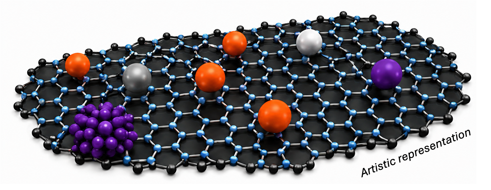
The microwave plasma environment can simultaneously drive N-graphene formation, nanoparticle generation, surface functionalisation, multiphase formation and nanoparticle anchoring onto the graphene scaffold. These concurrent processes create hierarchical hybrid structures and control nanoscale interfaces within one integrated synthesis environment.
From plasma parameters to measured electromagnetic performance
Plasma parameters → N-graphene chemistry, defects and interfaces → particle size, distribution and phase → dielectric and magnetic response → impedance matching and attenuation → reflection, transmission and absorption.
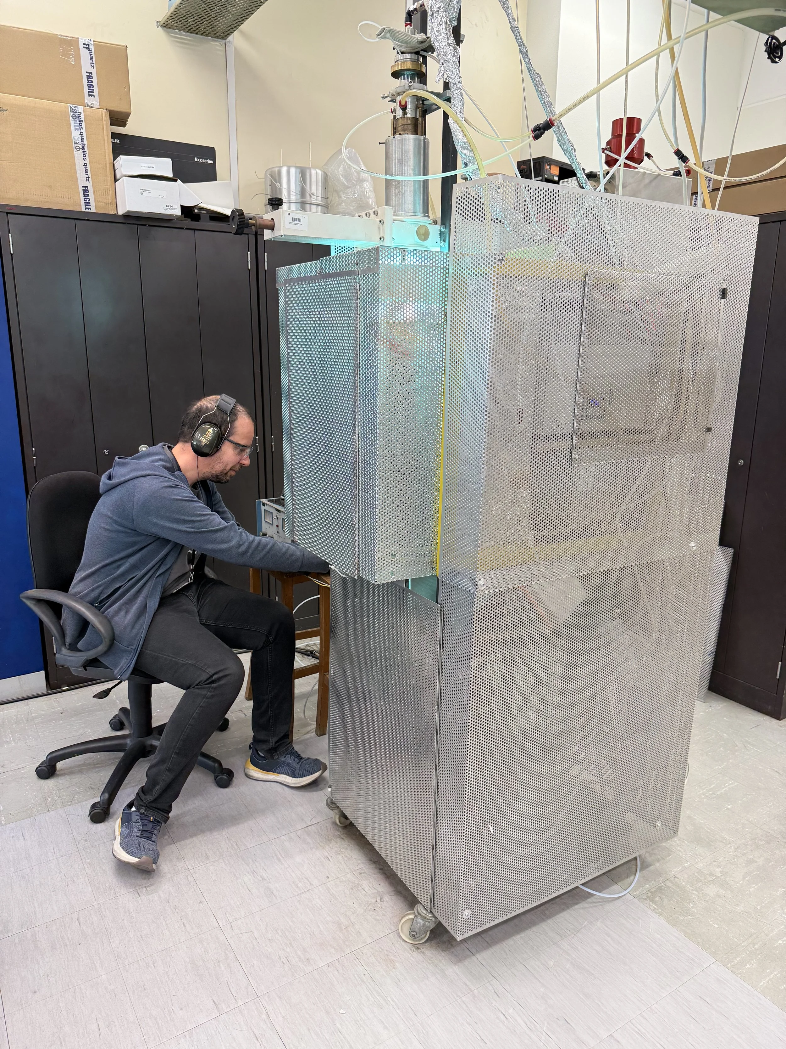
This chain connects synthesis directly to performance: plasma control shapes the nanostructure, the nanostructure determines the relevant electromagnetic properties, and calibrated measurements establish how the resulting material partitions incident power.
Define the electromagnetic requirement, including frequency range, maximum transmission, allowable reflection, geometry, environment and integration constraints.
Select or tailor the graphene material, including morphology, defect state, doping and functionalisation appropriate to the intended matrix and process.
Design the architecture by controlling loading, dispersion, interfaces, porosity, layers, gradients and, where justified, complementary dielectric or magnetic phases.
Measure scattering parameters and relevant constitutive properties over the required range, using representative specimens and a documented calibration method.
Iterate the composition and architecture against the application target, then validate the integrated component rather than relying only on coupon data.
GTechPlasma is therefore positioned as a plasma-enabled materials-engineering platform. The graphene is not treated as a commodity additive whose conductivity alone determines performance; its chemistry, nanostructure, interfaces and complementary phases are engineered as part of the complete electromagnetic material architecture.
AEGIS electromagnetic materials
From plasma synthesis to absorption-dominated electromagnetic shielding
AEGIS stands for Advanced Electromagnetic Graphene-based Shields via Plasma Induced Synthesis. Developed through work associated with the NATO Science for Peace and Security Programme, AEGIS is GTechPlasma’s platform for lightweight graphene-based materials engineered for electromagnetic shielding and absorption.
Conventional electromagnetic shielding often relies predominantly on high electrical conductivity to reflect incident electromagnetic energy. AEGIS takes a different approach. Its materials are designed to allow a substantial fraction of incident energy to enter the tested structure and then dissipate that energy through controlled electrical, dielectric, interfacial and, where applicable, magnetic loss mechanisms.
Tunable by formulation, not just thickness
Broadband electromagnetic response is often adjusted by changing absorber thickness or filler loading. GTechPlasma adds another design dimension by engineering N-graphene chemistry, defects, interfaces and complementary phases.
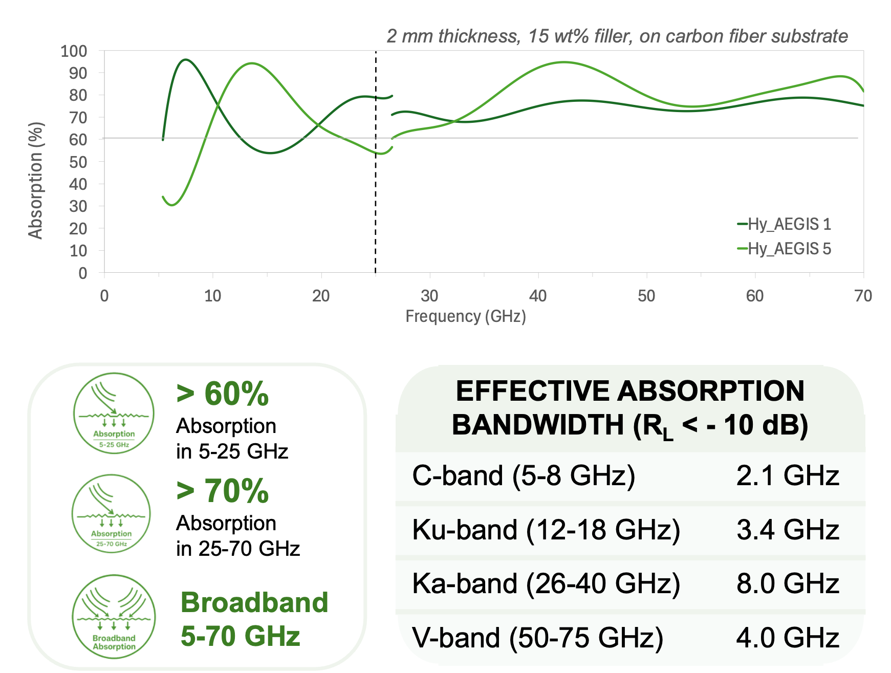
GTechPlasma’s different N-graphene hybrid formulations produced distinct electromagnetic responses while maintaining the same 2 mm specimen thickness and 15 wt% filler content. This demonstrates that absorption behaviour can be shifted through nanostructure and formulation design rather than relying only on changes in thickness or filler loading.
At these common conditions, one tested formulation produced an effective absorption bandwidth of approximately 2.1 GHz in the C band. A second formulation produced EAB values of approximately 3.4 GHz in Ku, 8 GHz in Ka and 4 GHz in V.
Why it works
Controlled electrical transport. Graphene and N-graphene networks provide conduction and resistive-loss pathways without requiring conductivity to be maximised at the expense of impedance matching.
Dipolar and interfacial polarisation. Nitrogen configurations, defects, functional groups and heterogeneous interfaces introduce polarisation centres and frequency-dependent dielectric-relaxation pathways.
Complementary functional phases. Additional phases can be selected to modify dielectric contrast, interfacial polarisation, eddy-current-related loss and magnetic-resonance mechanisms.
Engineered interfaces and nanostructure. Particle size, distribution, phase composition and attachment to the graphene scaffold influence the combined dielectric and magnetic response.
Absorption-oriented architecture. Loading, dispersion, thickness, porosity, layering and substrate conditions are engineered together to control energy entry, propagation and dissipation.
These mechanisms are combined according to the target electromagnetic response.
A plasma-enabled materials-engineering platform
AEGIS demonstrates the central GTechPlasma proposition: electromagnetic performance can be engineered through control of graphene chemistry, nanoscale interfaces, complementary phases and material architecture.
Rather than offering one universal composition, GTechPlasma develops tunable formulations for defined electromagnetic environments and integration requirements. The result is a platform for absorption-dominated shielding, electromagnetic compatibility, lightweight functional coatings and electromagnetic-signature materials—supported by measured performance and clearly stated claim boundaries.
Explore the AEGIS Technology
From plasma synthesis to absorption-dominated electromagnetic shielding: explore the GTechPlasma technology platform, material engineering approach and broadband performance in a single technical overview.
View AEGIS Technical Overview — PDF
Radar absorption, reflection loss and the path to RCS validation
Measurement metrics and equations
Scattering parameters and power coefficients
$$ \begin{aligned} R &= \left|S_{11}\right|^2 \\ T &= \left|S_{21}\right|^2 \\ A &= 1 - R - T \end{aligned} $$
These relations apply to a calibrated two-port measurement when the S-parameters are referenced consistently and the measured modes capture the relevant reflected and transmitted power. Fixture loss, leakage, higher-order modes, anisotropy and calibration residuals may require additional treatment.
Measured using vector network analysis
Complex S-parameters are measured with vector network analysers and appropriate waveguide or free-space configurations. The calibrated measurements are used to derive R = |S11|², T = |S21|² and A = 1 − R − T under the stated convention. Measurement geometry, reference planes, gating or other corrections, specimen thickness and uncertainty should accompany quantitative results.
Shielding effectiveness terms
$$ \begin{aligned} SE_T &= -10\log_{10}(T) \\[4pt] SE_R &= -10\log_{10}(1-R) \\[4pt] SE_A &= -10\log_{10}\left(\frac{T}{1-R}\right) \end{aligned} $$
With these definitions, $ SE_T = SE_R + SE_A $. The equations are useful for consistent reporting, but $ SE_A $ is conditional on the power that was not initially reflected. It is therefore different from the absolute absorbed fraction A. A material may show a large $ SE_A $ value even when a substantial part of the incident power is reflected.
Effective absorption
$$ A_{\mathrm{eff}} = \frac{A}{1-R} $$
$ A_{eff} $ describes the fraction absorbed from the power that enters the specimen after front-surface reflection. It can help analyse internal attenuation, but it must not be presented as the absorbed fraction of total incident power. Publish A and R alongside $ A_{eff} $.
Reflection loss for a metal backed absorber
$$ RL = 20\log_{10} \left| \frac{ Z_{\mathrm{input}}-Z_{\mathrm{free\ space}} }{ Z_{\mathrm{input}}+Z_{\mathrm{free\ space}} } \right| $$
Reflection loss is commonly used for metal-backed microwave absorbers. More negative values indicate less reflected field at the measurement plane under the stated configuration. RL is not interchangeable with EMI shielding effectiveness: a metal backing already suppresses transmission, so the measurement addresses reflection and absorption in that backed system.
| Metric | What it answers | Do not infer |
|---|---|---|
| SET | How strongly transmission is reduced. | How much incident power was absorbed. |
| R | What fraction of incident power is reflected. | Transmission attenuation by itself. |
| A | What fraction of incident power is absorbed. | Performance at another thickness or backing condition. |
| Aeff | What fraction of accepted power is absorbed. | Absolute absorption of the incident wave. |
| RL | How much field is returned by a stated absorber configuration. | Shielding effectiveness of an unbacked enclosure or sheet. |
| Topic | EMI shielding | Radar-absorbing materials and RCS work |
|---|---|---|
| Primary objective | Reduce transmission or coupling into or out of a protected region. | Reduce reflected energy or the radar signature of an integrated object. |
| Common specimen metric | SET with R, A and T. | Reflection loss or reflectivity under defined backing and incidence conditions. |
| System metric | Emissions, susceptibility, transfer impedance or enclosure shielding effectiveness. | Radar cross section as a function of frequency, aspect, polarisation and configuration. |
| Role of metal backing | May be part of an enclosure but changes the measured structure. | Common in absorber testing; it forces T toward zero and makes reflection central. |
| Integration sensitivity | Seams, apertures, grounding, contacts and cable penetrations can dominate. | Shape, edges, gaps, coating uniformity, substrate and observation geometry can dominate. |
| Safe claim | “Reduced transmission by [value] under [method and conditions].” | “Reduced reflectivity or RCS by [value] under [method and conditions].” |
EMI shielding and radar absorbing materials
EMI shielding is not the same as radar absorption
EMI shielding primarily seeks to limit electromagnetic transmission through a material, component or enclosure over specified conditions. Radar-absorbing materials seek to reduce the energy returned toward a radar receiver in a relevant geometry, frequency band, polarisation and angle range. A highly conductive metal can provide excellent EMI shielding by reflection while remaining a poor radar absorber.
GTechPlasma develops materials relevant to both domains, but the claims, test methods and acceptance criteria should remain separate. Coupon-level absorption can inform radar-material development; it does not establish platform-level radar-cross-section reduction. RCS claims require representative integration and measurement or validated simulation.
Applications
Electronics and communications
Graphene-based coatings, films and composites may be evaluated for housings, partitions, flexible circuits, sensor packages and communication equipment where mass, thickness, corrosion resistance, formability or reflection control matters. The final design must also address electrical continuity, seams, connectors, thermal management and regulatory EMC requirements.
Aerospace and mobility
Lightweight composite architectures can be relevant to avionics housings, airframe substructures, unmanned systems and transport electronics. Qualification must consider temperature cycling, humidity, fluids, vibration, adhesion, fire behaviour and the effect of structural damage on electromagnetic performance.
Defence and security
Potential uses include protected electronics, communication systems, lightweight shielding and materials for electromagnetic-signature management. EMI shielding, electromagnetic absorption and radar-cross-section reduction must be specified and validated as separate requirements. GTechPlasma can support material development and characterisation without disclosing restricted application details or proprietary formulations on the public page.
Advanced infrastructure and scientific systems
Telecommunications hardware, high-frequency instruments, sensors, laboratories and specialised installations may require local field control or lightweight absorptive structures. Frequency, power level, near-field or far-field conditions and environmental exposure should be defined before material selection.
Coatings and composite integration
A coating route can add electromagnetic function to an existing substrate, while a bulk composite can distribute that function through the part. Coating performance depends on surface preparation, thickness control, adhesion, cure, conductivity continuity and environmental stability. Composite performance depends on dispersion, orientation, processing history and the integrity of the conductive and lossy network.
Technical frequently asked questions
Is graphene effective for EMI shielding
Graphene can contribute effectively to EMI shielding when it forms an appropriate network or architecture. Its electrical conductivity, aspect ratio, low density and interfacial area make it useful in films, coatings, porous structures and composites. Performance is not guaranteed by the material name. It depends on graphene quality, loading, dispersion, orientation, thickness, matrix, frequency and the test method. A technically useful data sheet should therefore report the complete specimen and measurement conditions together with SE_T, R, A and T.
Does graphene absorb or reflect electromagnetic radiation
It can do both. A highly conductive graphene network may create a strong impedance mismatch and reflect a large part of the incident power. Defects, interfaces, controlled conductivity and complementary loss phases can increase internal dissipation. Whether reflection or absorption dominates is determined by the full structure and frequency range, not by graphene in isolation. Direct power coefficients provide better evidence than relying only on logarithmic shielding terms.
What is absorption dominant EMI shielding
Absorption-dominant shielding describes a structure in which the absorbed fraction of incident power exceeds the reflected fraction over a stated range and configuration, while transmission remains acceptably low. The claim should be based on A and R, not simply on SE_A being larger than SE_R. Thickness, backing, calibration, frequency, angle and polarisation must be stated because each can change the power balance.
Is higher electrical conductivity always better
No. Higher conductivity can reduce transmission, but it can also increase front-surface reflection. If the objective includes low reflection, the design must balance conductivity with complex permittivity, permeability where relevant, thickness and architecture. The optimal conductivity is therefore specific to the frequency range and product requirement.
What is the difference between graphene and graphene oxide for shielding
Graphene oxide usually contains more oxygen functional groups and structural disorder than high-quality graphene. It is generally less electrically conductive but easier to disperse in some matrices and offers many polar sites. Reduced graphene oxide restores part of the conductive network while retaining defects and residual functional groups. None is universally superior: the choice depends on the required conductivity, dispersion, interfaces, processing route and loss balance.
How can nitrogen doping affect electromagnetic properties
Nitrogen incorporation can alter carrier concentration, bonding configuration, defects, local dipoles and complex permittivity. These changes may tune dielectric loss or improve impedance matching in a particular composite. The effect depends on nitrogen content and configuration, graphene structure, frequency and matrix, so it must be established by composition and electromagnetic measurements rather than assumed from the presence of nitrogen alone.
What determines an absorber frequency range
The operating band emerges from constitutive properties, thickness, layer sequence, backing, morphology and incidence conditions. Dielectric and magnetic relaxation, resonance, quarter-wavelength interference and distributed structural features can all shape the response. Broadband absorption generally requires multiple complementary mechanisms or a graded architecture. A band claim must always state the threshold used, such as RL below −10 dB, and the test configuration.
How does thickness affect absorption
Thickness changes the propagation distance and phase accumulated within the material. It can increase attenuation and shift interference conditions, moving absorption peaks to different frequencies. A thicker specimen is not automatically better, because impedance matching and phase can also deteriorate. Results should be published as frequency-dependent curves for identified thicknesses, and comparisons should not mix specimens without noting the difference.
Can graphene based shielding be applied as a coating
Yes, graphene can be incorporated into conductive or lossy coating systems. Practical performance depends on dispersion, rheology, substrate preparation, adhesion, cure, dry-film thickness, continuity and environmental durability. Coupon measurements should be followed by testing on the intended substrate and geometry, including seams and edges where these affect the shielding path.
How should shielding data be compared
Compare results only after aligning frequency range, thickness, density, filler content, specimen geometry, backing and method. A peak value from a metal-backed absorber cannot be compared directly with free-standing EMI shielding data. Where lightweight performance matters, report thickness and areal density alongside the original curves. Normalised figures of merit can support comparison but should never replace the measured result.
What is the difference between shielding and radar cross section reduction
Shielding effectiveness quantifies transmission attenuation through a material or enclosure. Radar cross section describes how strongly an object scatters energy back toward a radar under defined frequency, aspect and polarisation. An absorptive coupon can be relevant to RCS reduction, but platform shape, edges, gaps, substrate, coating application and observation geometry all influence the final result. A coupon result is therefore evidence for material behaviour, not proof of a platform-level RCS value.
Scientific evidence and references
1. Xia, Y., Gao, W. and Gao, C. A Review on Graphene-Based Electromagnetic Functional Materials: Electromagnetic Wave Shielding and Absorption. Advanced Functional Materials 32, 2204591 (2022). DOI or source
Why it matters: reviews multiscale design strategies for graphene-based shielding and absorption.
2. Jovanović, S. et al. A review on graphene and graphene composites for application in electromagnetic shielding. Graphene and 2D Materials 8, 59–80 (2023). DOI or source
Why it matters: provides an open review of graphene structures, composite routes and shielding mechanisms.
3. Peng, M. and Qin, F. Clarification of basic concepts for electromagnetic interference shielding effectiveness. Journal of Applied Physics 130, 225108 (2021). DOI or source
Why it matters: distinguishes shielding-effectiveness terms from actual reflected and absorbed power fractions.
4. Tatarova, E. et al. Plasma-Driven Tuning of Dielectric Permittivity in Graphene. Small 20, 2303421 (2024). DOI or source
Why it matters: reports tunable permittivity in plasma-synthesised nitrogen-doped graphene over 1–40 GHz.
5. Dias, A. I. A. et al. Plasma-enabled multifunctional platform for gram-scale production of graphene and derivatives. Applied Materials Today 36, 102056 (2024). DOI or source
Why it matters: documents a plasma platform for continuous graphene and derivative production.
6. Bundaleska, N. et al. Microwave Plasma-Driven Synthesis of Graphene and N-Graphene at a Gram Scale. Processes 13, 196 (2025). DOI or source
Why it matters: describes atmospheric-pressure, continuous synthesis and control of graphene and N-graphene properties.
7. ASTM International. ASTM D4935 Standard Test Method for Measuring the Electromagnetic Shielding Effectiveness of Planar Materials. DOI or source
Why it matters: provides a recognised method for planar-material shielding measurements within its applicable range and conditions.
8. IEEE Standards Association. IEEE 299 Standard Method for Measuring the Effectiveness of Electromagnetic Shielding Enclosures. DOI or source
Why it matters: addresses enclosure-level shielding measurements rather than material coupons.
Engineering how materials interact with electromagnetic waves
GTechPlasma combines plasma synthesis, graphene science and electromagnetic materials engineering to develop graphene-based materials with tailored electrical and dielectric properties and, where the architecture includes appropriate functional phases, a designed magnetic response. The aim is to control how electromagnetic energy enters, propagates through and is dissipated within a material.
GTechPlasma is positioned as a plasma-enabled materials-engineering platform that controls nanostructure and coupled loss mechanisms to tune how electromagnetic energy is admitted, dissipated and transmitted.
For customers, that means a development process built around the application: define the electromagnetic requirement, select and tailor the material, design the architecture, measure the response and validate the integrated component. Conductivity is one design variable. Verified electromagnetic performance is the outcome that matters.
Discuss your frequency range, geometry, environment and performance target with GTechPlasma.